Welcome to Weather-Above
How to make a printed circuit board from artwork to the finished circuit board for the home hobbyist


There are many circuit board systems for the hobbyist , I suggest reading about different techniques before deciding which one is best suited for your printer ,light source ,etching technique. If you have a laser printer use one of the other methods ,searching on uTube you will find lots of information using different techniques in making circuit boards , I am using an Epsom inkjet printer D150 ,for circuit boards which are UV pre- sensitised you could use an unncoated copper blank circuit board and spray a UV photosensitive laquer,there are sellers of this product on eBay. Start by using a printed circuit board design package, my favourite programme is DesignSpark this is free www.DesignSpark.com
Thank you Alan for pointing me to DesignSpark program, another favourite use the basic pcb design Circuit Wizard. www.new-wave-concepts.com
When I'm happy with the circuit board design I print it out using a special coated plastic film product code CS-IJF , this is supplied by Classicscreen Manufacturing for more information about this product please go to www.Classicscreen.co.uk , this film can be used to create film positives for the silk screen printing industry perfect solution for colleges and universities.
Depending on the type of inkjet printer you are using I would recommend doing a print test using different paper types and ink settings to achieve the optimum density of the black ink, exposing the image onto the circuit board I am using mercury vapour lamp 125 W whatever your UV source you will need to do an exposure test to find the optimum exposure time, this will depend on the distance from the light source and the power of the lamps/UV tubes/exposure box.
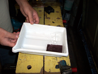
After you have exposed the film positive to the circuit board ,you then need to process the circuit board in a developer solution , you can buy this from Maplin electronics in powder, you would need to dissolve this into water please follow the instructions from the supplier importortant don't forget to wear plastic gloves and eye goggles before you start mixing the developer. You can use caustic soda 1 L of water then dissolve 10 g of caustic soda I would recommend doing a test to make sure you have the solution to the right strength when you place the circuit board into the developer solution oscillate the circuit board in the solution and it should start to dissolve away parts of the laquer you should be left with the image from the film positive and all the surrounding areas should be clear of lacquer it should take between 3~ 5 minutes to complete ,when the process is complete wash the circuit board in cold water leave to dry ,you can save the developer for another circuit board project save in a plastic bottle, make sure you are write on the plastic bottle what it contains and put it in a safe place away from children and animals etc.
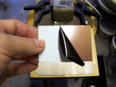
If you are using a pre-sensitised board there will be a light protective coating please peel away the coating before exposing to the UV light source.
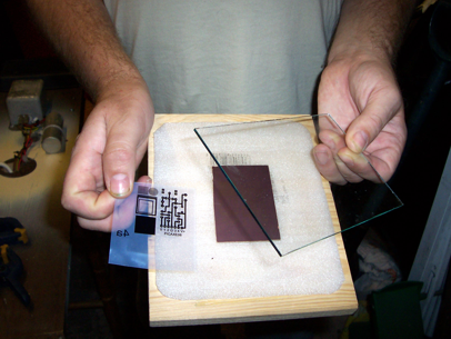
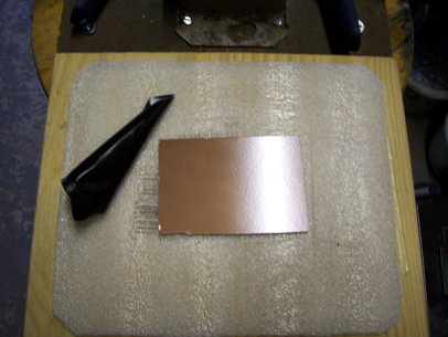
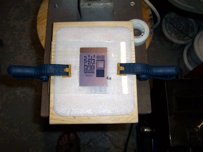
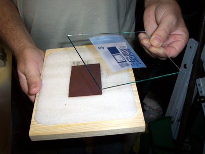
To keep the artwork film in contact with the circuit board I am using a block of wood with a very thin layer of foam /sponge material. After removing the protective coating I placed a circuit board on to the the foam then place the artwork positive film on top of the circuit board, to finish a glass plate is secured with two spring clamps which will compress all the layers together, this is called a contact board.
Photos of my lamp setup always look away from any uv light source,
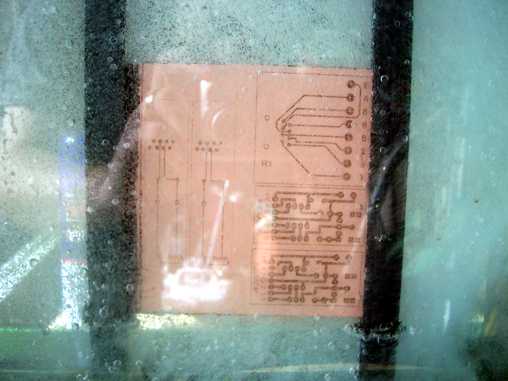
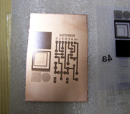
Circuitboard photos after the developing process has completed and washed in cold water then left to dry Inspect the image on the circuit board if there are any pin holds/faults in the image use a permanent marker pen to spot them out , any area that is copper will be removed during the etching process.
After exposure remove everything from the contact board
Please click on the images to enlarge
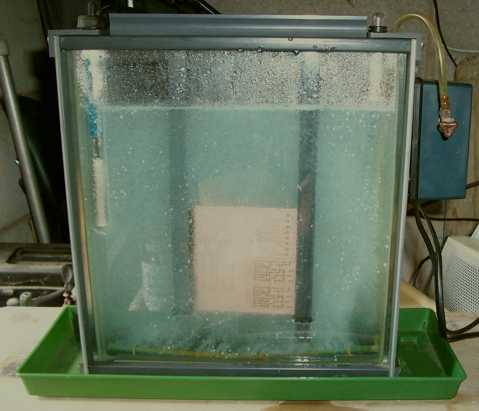
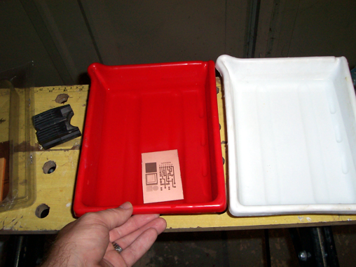
Mix up the etching crystals / powder, you can purchase this from Maplin Electronics , or from eBay suppliers,follow the information on the label. I have saved my chemicals and have made approximately 10 boards. Place a circuit board in the solution and oscillate in the solution until all the copper areas have been dissolved completely, this can take from 20 to 40 minutes depending on the temperature of the solution. When the etching process is complete remove the circuit board and wash in cold water and leave it to dry.
The next stage is to remove the lacquer from the circuit board,use acetone or nail varnish remover, this will reveal your copper tracks this is a good time to cut your circuit board, if needed, followed by drilling the small holes to accommodate your components.
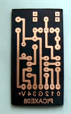
Finished etched circuit board
Printer settings for Epsom D120
using special coated plastic film
product code CS-IJF
Please click on the images to enlarge
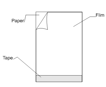
Printing Tip
Some standard inkjet printers have difficulty in feeding plastic coated films, to overcome this problem take a sheet of the A4 CS-IJF film lay this on top of a standard A4 piece of paper make sure you have the very slight tack facing up, this is the coated side to be printed on. Use some magic tape to stick the two pieces together , the edge you have taped together is the leading edge into your printer.